Testing scope: Non destructive testing of internal defects in metal and non-metal products and materials
Detection type: pores, cracks, inclusions
Search:
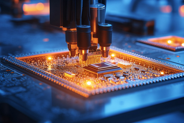
Using X-rays and CT to perform defect detection, structural observation, assembly inspection, and two-dimensional rapid inspection in integrated circuits and electronic manufacturing
Testing scope: Non destructive testing of internal defects in metal and non-metal products and materials
Detection type: pores, cracks, inclusions
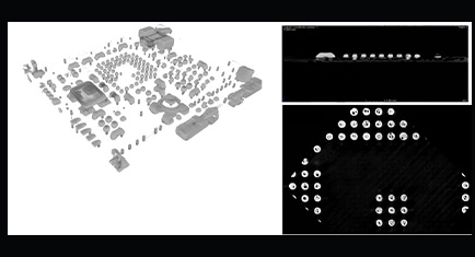
Restore the internal situation of the product to obtain a complete and three-dimensional dataset, in order to analyze sample defects and failure situations
Meet the micro nano detection needs of electronic components and promptly detect non-conforming parts in the early stage of pre production
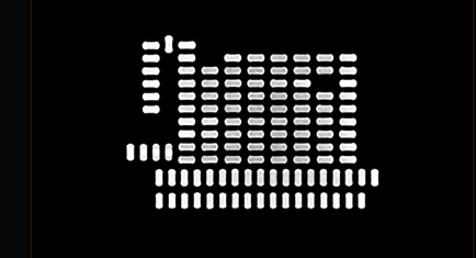
2D X-ray imaging: mainly used for PCB assembly defect detection, as it can simultaneously observe all layers of the PCB. This technology is non-destructive and allows for welding quality inspection of any component that cannot be inspected for solder joints through microscopy, AOI, or other "surface" testing methods. These components include but are not limited to BGA, LGA, and QFN. Therefore, 2D X-ray imaging is mainly used to search for solder bridging, solder voids, and calculate the area of solder voids.
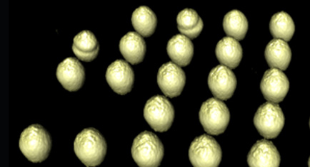
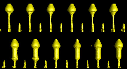
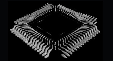
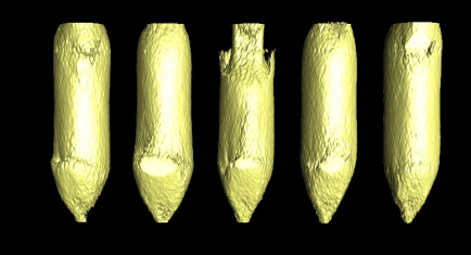
3D computed tomography (CT) imaging: used for qualitative and quantitative defect analysis of the entire PCB and its components. CT can independently analyze each layer of the PCB, thus detecting breaks, delamination, and other defects within the PCB itself. CT also allows for full 3D rendering of components and their internal workings, such as bonding wires. The CT process requires the sample to be clamped on the spindle and rotated 360 degrees while remaining above the X-ray tube, making it the most suitable for small, lightweight samples.
In the quality inspection of IC packaging, X-ray testing equipment is usually used to detect typical defect prone areas such as bonding wires, chip bonding, molding, and sealing. However, miniaturization, the use of new materials, and the increasing complexity of chips pose challenges for X-ray detection.
Miniaturization: The internal structure has a higher density and smaller size, such as micropores and flip chip interconnects, requiring sub micron resolution at the highest magnification, such as the new nano focus.
The use of new materials: The ordinary X-ray imaging effect of non-conductive chip adhesives or copper bonding wires is not good (high absorption materials: copper, steel, tin alloys, etc.)
Chip complexity, such as stacking, leads to confusing two-dimensional X-ray images. In IC packaging, the internal keys are flip chip solder joints, whose features and defects are similar to the known area array solder joints in electronic assembly. Appropriate image resolution is required to detect defects such as gaps and shape deviations within the micrometer range.
To solve these new problems, the future trend of IC packaging inspection is to use nano focal X-ray and high-resolution CT.